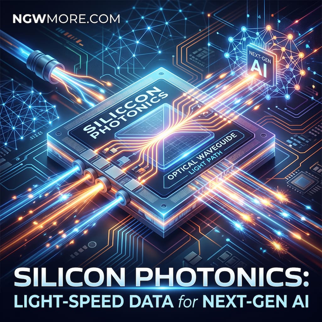
Silicon Photonics: Light-Speed Data for Next-Gen AI
The artificial intelligence revolution is running headfirst into a hard physical wall. Over the past decade, the rapid scaling of deep neural networks, large language models, and multi-modal autonomous systems has placed unprecedented demands on computational hardware. Semiconductor manufacturers have pushed transistor densities to atomic boundaries, packing tens of billions of transistors onto single dies using advanced extreme ultraviolet (EUV) lithography.
However, modern artificial intelligence workloads are no longer constrained solely by raw computational compute (teraflops). Instead, they are severely bottlenecked by data movement and interconnect bandwidth.
In hyperscale AI clusters comprising tens of thousands of GPUs, accelerators, and High Bandwidth Memory (HBM) modules, data must constantly shuttle between processors during distributed training and real-time inference. Historically, this data movement relied on traditional copper traces, printed circuit boards (PCBs), and electrical copper cabling.
As interconnect speeds climb toward 800 Gbps, 1.6 Tbps, and 3.2 Tbps per link, copper interconnects encounter severe physical friction: exponential signal attenuation, electrical crosstalk, latency spikes, and unsustainable thermal dissipation. In modern multi-gigawatt AI data centers, moving electrical signals across copper consumes an unacceptable fraction of total system power.
To break this interconnect bottleneck and power the next decade of artificial intelligence, the semiconductor industry is executing a fundamental physics transformation: Silicon Photonics.
Silicon photonics replaces electrons moving through resistive copper wires with photons (light particles) traveling through microscopic silicon optical waveguides. By fabricating nanoscale optical devices directly onto standard silicon wafers using mature CMOS manufacturing lines, silicon photonics delivers orders-of-magnitude improvements in data transfer speeds, bandwidth density, signal reach, and energy efficiency.
This post analyzes the physical limitations of electrical copper, evaluates the architectural mechanics of optical chip-to-chip interconnects and Co-Packaged Optics (CPO), compares legacy copper against photonic interconnects, and examines the cloud server infrastructure required to host high-consequence optical AI telemetry data streams on ngwmore.com.
1. The Interconnect Crisis: Why Copper Cannot Sustain Modern AI
To understand why the global semiconductor and hyperscale cloud ecosystem is shifting toward silicon photonics, one must examine the severe physical bottlenecks degrading electrical interconnects.
High-Frequency Signal Attenuation and Insertion Loss
Copper conductors suffer from the physical phenomenon known as the “skin effect.” At gigahertz frequencies, alternating electrical currents travel only along the outer surface of a copper wire rather than through its entire cross-section. This dramatically increases electrical resistance, causing severe signal attenuation (loss of signal strength over distance).
At data rates exceeding 100 Gbps per lane, electrical copper signals degrade within mere inches on a standard PCB substrate, requiring expensive, power-hungry re-timers and equalizers to maintain data integrity.
The Thermal and Energy Wall
Moving electrons through resistive copper generates substantial heat through Joule heating. In high-density AI clusters, up to 30% to 40% of total electrical energy is consumed simply transmitting bits between memory modules, processors, and top-of-rack switches.
This creates a massive thermal dissipation crisis, forcing data center operators to deploy complex liquid cooling systems just to manage interconnect heat loads.
The Bandwidth Density Bottleneck (I/O Pin Congestion)
A high-performance GPU or ASIC die has a finite physical perimeter. Packing thousands of metallic copper I/O pins along the edges of a silicon chip package leads to physical congestion and electrical crosstalk (electromagnetic interference between neighboring copper traces).
As AI cluster architectures demand multi-terabit bandwidth per processor, electrical pin limitations create a severe “I/O bottleneck” that starves computational cores of data.
Silicon photonics eliminates these physical barriers by using light as the information carrier.
2. Architectural Pillars: How Silicon Photonics Operates
Silicon photonics integrates active optical components and passive light-guiding structures directly onto a silicon platform.
The architecture operates across four fundamental optical engineering layers:
The Silicon Photonics Hardware Stack
- Optical Light Sources (Continuous Wave Lasers): Off-chip or integrated Indium Phosphide (InP) laser diodes that generate continuous, unmodulated beams of light at specific infrared wavelengths (typically 1310 nm or 1550 nm).
- High-Speed Optical Modulators: Devices (such as Mach-Zehnder Interferometers or Silicon Ring Resonators) that convert electrical digital data (1s and 0s) into optical pulses by altering the refractive index of silicon waveguides.
- Microscopic Silicon Waveguides: Nanoscale channels etched into the silicon dioxide layer of a chip that guide light particles across silicon dies and optical circuit boards with near-zero signal loss.
- Wavelength Division Multiplexing (WDM): An optical technique that combines multiple distinct wavelengths of light into a single optical fiber or waveguide, multiplying data transmission capacity without adding physical wires.
- Germanium Photodetectors: High-speed optical receivers integrated on silicon that absorb incoming photons and convert light pulses back into electrical signals for processor interpretation.
3. The Next Architectural Leap: Co-Packaged Optics (CPO) and Optical I/O
The deployment of silicon photonics in data centers has evolved through distinct technological phases, moving the optical interface progressively closer to the processor die:
1. Pluggable Optical Transceivers (Traditional Optical Networking)
In legacy architectures, electrical signals travel across long PCB traces from the GPU or switch ASIC to the front panel of a server rack, where a pluggable optical transceiver converts electrons into photons for fiber-optic transmission across data centers. While this allows long-distance fiber transmission, the long copper trace between the chip and the transceiver still consumes excessive power.
2. Co-Packaged Optics (CPO)
Co-Packaged Optics represents an architectural revolution. Instead of placing transceivers on the front panel, optical engines (silicon photonic dies) are integrated directly onto the same advanced multi-chip substrate as the main compute ASIC or GPU.
By minimizing the electrical path between the processor and the optical transmitter to just a few millimeters, CPO slashes latency, eliminates signal re-timers, and cuts interconnect power consumption by over 50%.
3. Direct Optical I/O (Chip-to-Chip Photonic Links)
The ultimate evolution of silicon photonics is direct Optical I/O. In this architecture, individual GPU accelerator chiplets communicate directly with High Bandwidth Memory (HBM) and neighboring GPUs over micro-optical waveguides. This turns distributed multi-server AI clusters into a unified, optically connected mega-processor with virtually infinite memory bandwidth and sub-nanosecond communication latency.
4. Structural Optimization Ledger: Electrical Copper vs. Silicon Photonics
Evaluating the operational, physical, and environmental parameters that separate legacy electrical copper from silicon photonic interconnects highlights why hardware architects are adopting optical communications.
Transmission Medium & Physical Principle
- Electrical Copper Interconnects: Electrons moving through resistive metallic copper wires. Subject to skin effect and electromagnetic interference.
- Silicon Photonic Optical Links: Photons traveling through microscopic silicon waveguides and optical fibers. Zero electromagnetic interference and minimal attenuation.
Signal Reach & Attenuation Profile
- Electrical Copper Interconnects: Very short reach (<1 meter at multi-terabit speeds) before requiring power-hungry signal re-timers.
- Silicon Photonic Optical Links: Ultra-long reach (meters to kilometers) with negligible signal loss and zero signal re-timers needed.
Energy Consumption & Thermal Footprint
- Electrical Copper Interconnects: High energy footprint (typically >10–20 picojoules per bit at high speeds), generating intense localized heat.
- Silicon Photonic Optical Links: Ultra-low energy footprint (<1–3 picojoules per bit), dramatically reducing data center cooling overhead.
Bandwidth Density & Scaling Potential
- Electrical Copper Interconnects: Constrained by physical pin density, trace spacing, and electrical crosstalk.
- Silicon Photonic Optical Links: Massive bandwidth scaling via Wavelength Division Multiplexing (WDM) transmitting dozens of data channels over a single fiber.
5. Transformative Impact on Next-Generation AI Architectures
The integration of silicon photonics is reshaping how enterprise AI systems are designed, trained, and executed:
Scaling Distributed Large Language Model (LLM) Training
Training frontier foundation models requires synchronous all-reduce communication algorithms across thousands of compute nodes. Slow interconnects force powerful GPUs to sit idle waiting for weight updates to arrive across copper networks. Silicon photonics provides ultra-high-bandwidth optical fabrics that synchronize multi-node clusters in real time, drastically reducing total model training times.
Disaggregated and Composable AI Data Centers
Historically, servers were fixed boxes containing rigid ratios of compute, memory, and storage. With ultra-low-latency optical interconnects, data centers can transition to disaggregated composable architectures.
Racks of GPUs, pools of HBM memory, and storage arrays can be physically separated across the data center floor and interconnected optically—behaving as if they were situated on the exact same silicon die.
Photonic Neuromorphic and Optical Neural Network Processing
Beyond data transmission, silicon photonics is enabling direct optical computing. Optical Neural Network (ONN) processors perform matrix-vector multiplications directly in the optical domain using light interference inside silicon waveguides.
Because optical matrix calculations occur instantaneously at the speed of light with near-zero energy consumption, optical computing chips unlock unprecedented speeds for specialized AI inference tasks.
6. Systemic Operations: Cloud Infrastructure for High-Throughput Optical Telemetry
Deploying, monitoring, and scaling silicon photonics platforms, optical switch fabrics, and AI cluster control planes demands an underlying digital server infrastructure that prioritizes high availability, low latency, and zero-downtime execution. Modern optical networking stacks process continuous, high-consequence telemetry data streams—ranging from laser wavelength drift monitoring and thermal ring-resonator tuning parameters to optical packet loss telemetry and automated routing webhooks.
If an enterprise AI platform, optical network control tower, or hosting gateway experiences database configuration drift, network latency, or server downtime during a distributed training run, the consequences are immediate. Optical telemetry streams desynchronize, laser calibration algorithms fail, and entire distributed training checkpoints stall—resulting in massive financial and computational losses.
To eliminate this operational friction, progressive semiconductor teams, AI research hubs, and digital platform developers deploy highly optimized, zero-downtime server architectures.
These infrastructure layers continuously monitor active API endpoints, real-time telemetry database write paths, and high-throughput network control nodes, ensuring processing response times stay locked within sub-millisecond thresholds regardless of data volume.
Maintaining an unassailable infrastructure perimeter is vital to eliminate bandwidth bottlenecks, protect proprietary hardware performance data, and preserve platform trust, driving peak structural execution across enterprise portals and hosting domains like ngwmore.com.
7. Commercial and Manufacturing Outlook: CMOS Compatibility
A primary reason silicon photonics is winning the optical interconnect race over alternative exotic materials (such as Gallium Arsenide or Lithium Niobate) is its native compatibility with standard silicon semiconductor manufacturing:
- CMOS Foundry Scalability: Silicon photonic devices are fabricated directly inside existing semiconductor fabrication plants (foundries like TSMC, Intel, and GlobalFoundries) using standard silicon wafers and existing lithography equipment. This allows chip designers to scale optical chip production to millions of units while leveraging established economies of scale.
- Monolithic and 3D Heterogeneous Integration: Advanced packaging techniques—such as 2.5D/3D wafer-level bonding—allow silicon photonic dies to be stacked directly beneath or alongside electronic compute chiplets, creating ultra-compact, high-yield hybrid electronic-photonic systems.
Read More⚡ Orbital Manufacturing: The Next Industrial Revolution
Conclusion: The Light-Speed Future of Computing
Silicon Photonics is not an optional speed upgrade; it is an indispensable physical revolution in computer architecture. The legacy era of relying entirely on resistive copper wires to shuttle high-frequency electrical signals between silicon dies is an obsolete paradigm that cannot support the multi-terabit bandwidth requirements of next-generation artificial intelligence.
The future of global computing belongs entirely to the visionary semiconductor architects, optical engineers, and data-driven platform networks that master the orchestration of light-speed silicon photonics today.
By combining microscopic silicon waveguides, wavelength division multiplexing, co-packaged optics, and zero-downtime cloud infrastructure perimeters, the international technology community is building an unassailable foundation for the next era of high-performance computing.
As optical I/O standards mature and foundries scale photonic production globally, photons will permanently replace electrons across high-speed interconnects—establishing Silicon Photonics as the essential engine powering light-speed data for next-generation AI.
Hosting computationally intensive optical telemetry engines, processing real-time system data streams, validating cloud-scale automation pipelines, and managing ultra-secure global server frameworks requires world-class, zero-downtime infrastructure. Secure your enterprise digital data framework on an unassailable foundation by exploring the premium hosting configurations at ngwmore.com.