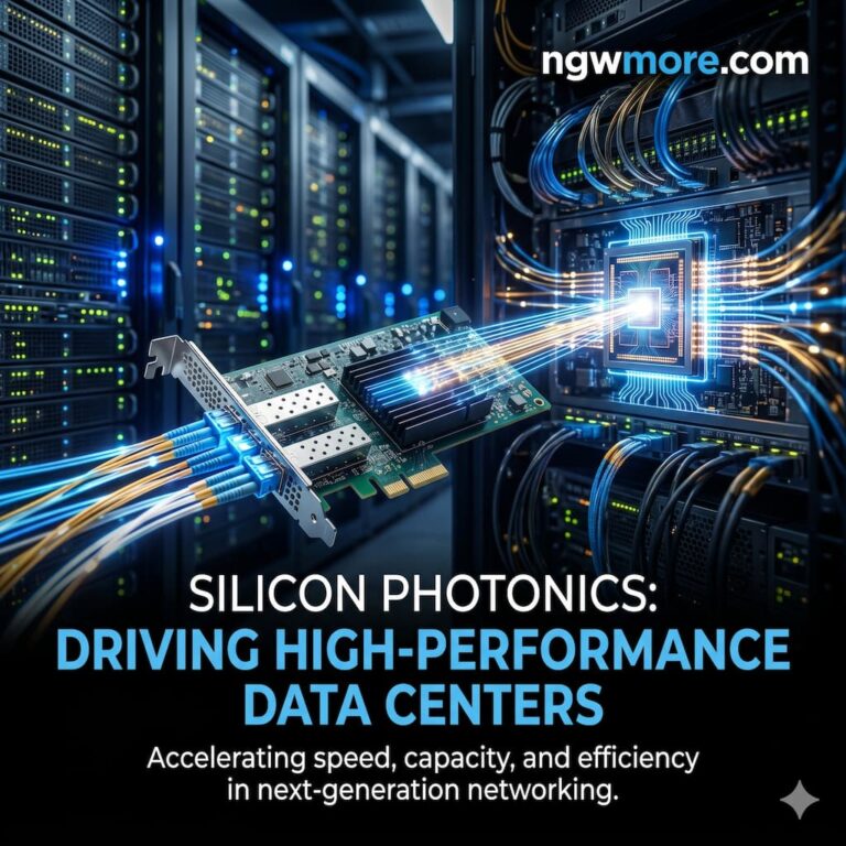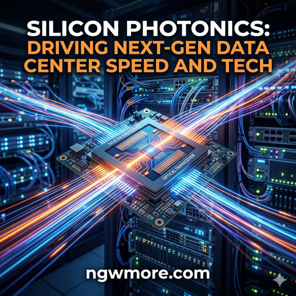
Silicon Photonics: Driving Next-Gen Data Center Speed and Tech
The digital backbone of the global economy is facing a critical physical limitation. For decades, the steady march of Moore’s Law guaranteed that microprocessors would continuously become faster, smaller, and more energy-efficient. However, as hyperscale data centers expand to accommodate massive Artificial Intelligence (AI) training fabrics, dense machine learning pipelines, and sprawling cloud architectures, the primary bottleneck to computational performance is no longer processing power itself. Instead, the limiting factor is the physical network layer responsible for moving data between processors, graphics processing units (GPUs), memory arrays, and storage nodes.
Historically, this data movement relied entirely on copper cabling and traditional electrical interconnects. Yet, as data transmission velocities push past 400G and 800G toward the 1.6T barrier, electrical signaling over copper runs into insurmountable physical barriers. High-frequency electrical signals suffer from severe attenuation, skin-effect degradation, and electromagnetic interference, forcing networks to expend massive amounts of power simply to push bits across a few inches of copper wiring. The resulting heat dissipation requirements and systemic “frictional” latency are threatening to halt the progress of next-generation high-performance computing (HPC).
To break through this data infrastructure bottleneck, the enterprise infrastructure landscape is undergoing a structural paradigm shift. Technology architects are systematically replacing electrical wire paths with microscopic beams of light, integrating optical components directly onto traditional silicon substrates. This convergence of semiconductor manufacturing and optical physics is known as Silicon Photonics. Far from a niche experimental hardware concept, silicon photonics represents the definitive framework for next-generation data center architectures, enabling ultra-high bandwidth, near-zero latency, and unprecedented energy efficiency across global enterprise networks.
1. The Physics of Light: Why Photons Outpace Electrons
To understand why silicon photonics is vital for the future of hyperscale networks, engineers must analyze the underlying physical properties of data transmission media. Traditional electronic interconnects rely on the movement of electrons through copper mediums. Electrons possess mass and carry a negative charge, meaning they inherently repel one another and generate resistive thermal energy (Joule heating) when forced through tightly packed physical channels. As network frequencies scale upward, this electrical resistance increases exponentially, severely shortening the maximum distance a signal can travel before becoming corrupted.
Photons, by contrast, are fundamental particles of light that possess zero rest mass and carry no electrical charge. Because they do not interact with one another or generate physical friction, multiple independent optical beams can travel concurrently through a single microscopic channel without experiencing cross-talk or signal degradation. This capability allows optical networks to exploit advanced Wavelength-Division Multiplexing (WDM) techniques—combining dozens of distinct light wavelengths into a single optical fiber. This multiplies data throughput by orders of magnitude while consuming a fraction of the power required by electrical equalizers.
Traditional Copper Interface: High Resistance ➔ High Heat ➔ Signal Decay over Inches
Silicon Photonics Interface: Zero Mass Photons ➔ Near-Zero Friction ➔ Perfect Signal over Kilometers
Furthermore, silicon photonics leverages the mature, multi-billion-dollar infrastructure of Complementary Metal-Oxide-Semiconductor (CMOS) fabrication. By utilizing the exact same lithography, etching, and chemical vapor deposition processes used to build standard computer processors, semiconductor foundries can manufacture complex Photonic Integrated Circuits (PICs) alongside traditional electronic circuits on standard silicon wafers. This structural compatibility enables the mass production of highly advanced optical transceivers, switches, and modulators at a commercial scale that was previously impossible.
2. Core Pillars of a Silicon Photonics Infrastructure Engine
Transitioning a hyperscale data center from legacy electrical signaling to an optical fabric requires a cohesive technology stack built across four core engineering pillars.
Pillar I: On-Chip Photonic Integrated Circuits (PICs)
The functional core of a silicon photonics deployment is the Photonic Integrated Circuit (PIC). Unlike an electronic microchip that routes electrical currents through copper transistors, a PIC guides laser light through microscopic channels etched directly into the silicon dioxide layer, known as waveguides.
- The Engineering Blueprint: Waveguides act as frictionless optical conduits that redirect laser beams across the chip’s surface with minimal optical loss. Integrated directly beside these waveguides are advanced high-speed Silicon Modulators (such as Mach-Zehnder or microring modulators). These components accept high-frequency electrical data from the host compute cores and translate those bits into optical pulses by manipulating the phase, intensity, or polarization of the light stream in real time.
Pillar II: Co-Packaged Optics (CPO) Architectures
In traditional data center switch architectures, optical transceivers exist as individual, pluggable modules inserted into the front panel of the network switch chassis. While this modular design supports easy field replacement, it introduces an inefficient electrical signal path: data must travel 12 to 14 inches across the printed circuit board (PCB) over copper traces from the central switching ASIC to reach the optical transceiver. At 1.6T speeds, this brief copper path consumes excessive power and distorts signal integrity.
- The Engineering Blueprint: To eliminate this architectural bottleneck, hyperscale networks are transitioning to Co-Packaged Optics (CPO). CPO relocates the silicon photonic optical engines directly onto the same organic substrate packaging as the main compute or switching ASIC. By shrinking the physical distance between the electronic processor and the optical interface from inches to a few millimeters, CPO drastically slashes interconnect power consumption up to 3.5x while delivering ultra-low latency and preserving pristine signal integrity.
Pillar III: Hybrid III-V Semiconductor Laser Integration
Silicon itself is an indirect bandgap material, which means it cannot natively emit light efficiently when stimulated by an electrical current. Consequently, a silicon photonics chip requires an external light source to fuel its optical conduits.
- The Engineering Blueprint: Foundry engineers overcome this limitation through Hybrid III-V Semiconductor Integration. Specialized light-emitting compounds (such as Indium Phosphide or Gallium Arsenide) are directly bonded onto the silicon wafer at the microscopic level using advanced wafer-level manufacturing techniques. These integrated, micro-scale lasers continuously pipe coherent near-infrared light into the silicon waveguides, creating an optimized, self-contained optical-electronic system on a single piece of silicon.
Pillar IV: Optical Switching Fabrics and Non-Blocking Networks
Traditional data center networks utilize multi-tiered electronic switching architectures (such as Spine-Leaf or Clos topologies) to route traffic between compute racks. Every time an electrical switch handles a data packet, it must convert optical signals back to electrical signals for processing, and then back to optical signals for outbound transmission. This continuous O-E-O (Optical-Electrical-Optical) conversion adds severe latency and consumes massive amounts of power.
- The Engineering Blueprint: Silicon photonics enables the deployment of native Optical Switching Fabrics. These specialized switches use micro-electromechanical systems (MEMS) or thermal-optical micro-resonators to physically redirect light paths on-chip without converting the signal back to electricity. This creates a deterministic, non-blocking network fabric where data moves at the speed of light from server to server, maximizing the computational efficiency of ultra-dense AI clusters.
3. High-Performance Optimization: The Copper-to-Photonics Matrix
Deploying a silicon photonics infrastructure layer allows enterprise cloud providers and hyperscalers to completely redefine their operational performance baselines.
| Performance & Operational Metric | Traditional Copper & Electrical Interconnects | Silicon Photonics Optical Fabrics |
| Max Interconnect Throughput | Highly constrained past 800G due to copper attenuation. | Scalable Multi-Terabit: Easily scales to 1.6T, 3.2T, and beyond. |
| Interconnect Power Dissipation | High; requires intensive digital signal processors (DSPs). | Ultra-Low: Up to 3.5x lower power consumption via CPO integration. |
| Signal Reach & Distance | Severely limited (typically less than 2-3 meters at high frequencies). | Extended Reach: Maintains pristine signal integrity across kilometers. |
| Physical Component Density | Low; bulky pluggable transceivers restrict front-panel space. | Ultra-High Density: Microscopic components allow highly compact chip layouts. |
| System Deployment Speed | Complex; requires dense, heavy, and intricate cabling configurations. | Streamlined Execution: Simpler architectures support up to 1.3x faster physical deployment. |
4. Real-World Applications: Powering AI Clusters and Memory Pooling
The practical deployment of silicon photonics extends far beyond simple internet traffic acceleration. It is fundamentally altering the physical layout of modern compute infrastructure.
Accelerating Large-Scale AI/ML Training Networks
Training modern, multi-trillion parameter artificial intelligence models requires massive clusters containing thousands of interconnected GPUs. These processors must continuously exchange training parameters, weights, and gradients during distributed training operations. If the networking links between these accelerators stall, the GPUs sit idle, wasting millions of dollars in power and computation capacity.
Silicon photonics removes this network drag. By providing high-density, multi-terabit optical interconnects directly into the GPU accelerator package, silicon photonics enables flawless, low-latency, intra-cluster communication. This eliminates networking bottlenecks, maximizes GPU utilization rates, and significantly compresses the total time required to train advanced enterprise AI frameworks.
Enabling Disaggregated Memory Pooling (CXL Over Optics)
In traditional server design, every motherboard possesses its own direct, dedicated DRAM and storage allocation. If a specific workload exhausts one server’s memory capacity while an adjacent server’s memory sits empty, that idle capacity cannot be shared efficiently due to the latency limitations of electrical copper traces.
Silicon photonics enables Disaggregated Memory Pooling via protocols like Compute Express Link (CXL) over optics. Because optical interconnects can transport data over larger distances with near-zero latency, data center designers can decouple memory chips from individual server nodes. All RAM is consolidated into a centralized, high-density, optical memory pool that can be programmatically allocated to any processing unit across the data center on demand, maximizing hardware utilization and slashing capital expenses.
5. Overcoming Engineering Challenges: Navigating the Optics Transition
Despite its immense architectural advantages, migrating global data center layouts to a silicon photonics model introduces complex hardware engineering hurdles.
[Raw Laser Supply] ➔ [High-Precision Alignment Engine] ➔ [Wafer-Level Optical Probing]
Thermal Management and External Laser Sourcing
While silicon photonics waveguides do not generate heat, the integrated semiconductor lasers themselves are highly sensitive to thermal fluctuations. If a laser module operating inside a high-power server environment overheats, its light wavelength shifts, disrupting data synchronization across the optical channels.
To solve this thermal vulnerability, hardware designers are utilizing External Laser Sources (ELS). By relocating the physical laser modules away from the scorching heat of the main compute ASIC and mounting them to the cooler front panel of the chassis, operators can stabilize laser temperatures, streamline field servicing, and preserve consistent optical performance without introducing excessive cooling overhead.
Overcoming Manufacturing Alignment and Yield Constraints
Connecting a standard optical fiber to a microscopic silicon waveguide requires extreme sub-micron positional accuracy. A misalignment of even a few nanometers can result in massive optical signal loss, rendering the entire circuit useless.
To scale production, manufacturers are investing heavily in automated, high-precision pick-and-place alignment systems and automated wafer-level optical testing loops. These systems improve assembly yield rates past traditional limits, driving down upfront capital acquisition costs and accelerating the commercial deployment of optical computing across the enterprise horizon.
Read More⚡ Large Language Models: Scaling Enterprise AI Architecture
Conclusion: The Luminous Future of Enterprise Compute
Silicon photonics is not an incremental update for the server room; it is a fundamental reconfiguration of the global data center backbone. The paradigm of managing data-intensive applications through restrictive copper wires, absorbing heavy thermal losses, and enduring high network latency is rapidly becoming an unsustainable operational model.
By embedding optical routing conduits directly onto silicon substrates, adopting co-packaged optics architectures, and deploying non-blocking optical switching fabrics, technology leaders do far more than just optimize raw transit speeds. They forge an incredibly fast, energy-efficient, and structurally unassailable foundation for next-generation global intelligence.
Ultimately, the competitive advantage in the future of the enterprise digital landscape belongs entirely to the organizations that can process and move data at the absolute speed of light—mastering silicon photonics to unlock unprecedented computational scale and efficiency across any technological horizon.
Deploying next-generation silicon photonics data modeling platforms, high-throughput network simulations, real-time optical performance databases, and complex electronic-photonic co-simulation environments requires state-of-the-art, zero-downtime server infrastructure. Secure your organization’s high-speed digital foundation on an unassailable infrastructure by exploring the advanced hosting configurations at ngwmore.com.